NASR-M SYZYGY carrier board
NASR-M
Some time ago, I decided to try Xilinx Zynq, which everyone is using in their RF projects. And what is a better option for exploring a new chip than making a board around it? Spending some money on a reference design devkit from the manufacturer? No, that's certainly not my way of learning things.
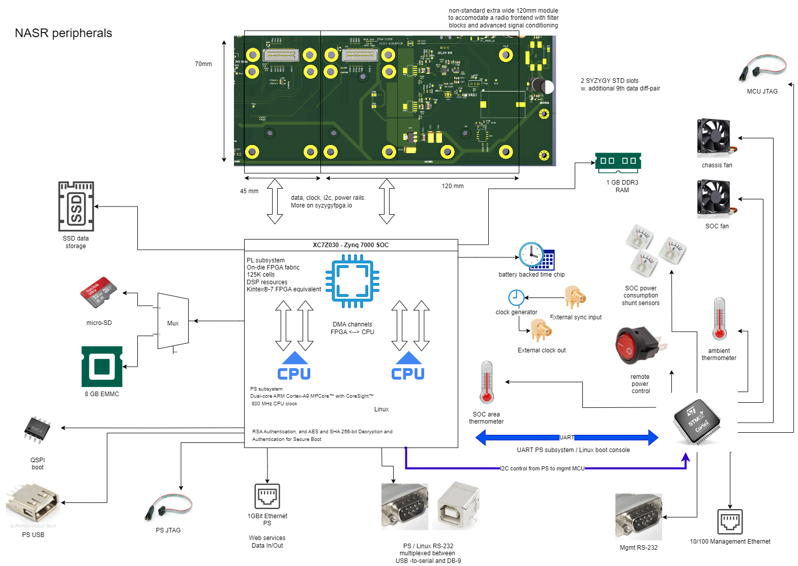
My dream board had 1GB of 32-bit-wide DDR3 RAM, SYZYGY ports, a standard ATX power supply, 1Gb ethernet port, and remote management that would allow me to flash firmware, control the system remotely, and export temperature and power usage readings to let me debug comfortably. Since that's my first rather complex embedded board in KiCad, I have made some dubious choices with PCB stackup, component placement, and routing. Sounds counterintuitive, but that was already a great learning experience in how not to do things and which design choices to avoid. It may work, however. I am pretty concerned about the DDR3 part, which was the most challenging part to route.
But if it works, I would have an excellent opportunity to play with software radio on a different level. And by different level, I mean a system built from scratch. Long story short, it's on a GitHub, completely open "with open-source everything". Once the board boots up, I will publish the Vivado design and the board MCU firmware sources. This will take some time, though. Once I'm more confident in design, I'll order PCBs from JLCPCB, and it will take even more time to solder the components in circuit by circuit, starting with the MCU, then the secondary PSU, and the rest. Scroll down into the long list of things that could break if you are interested in this rather dramatic development.
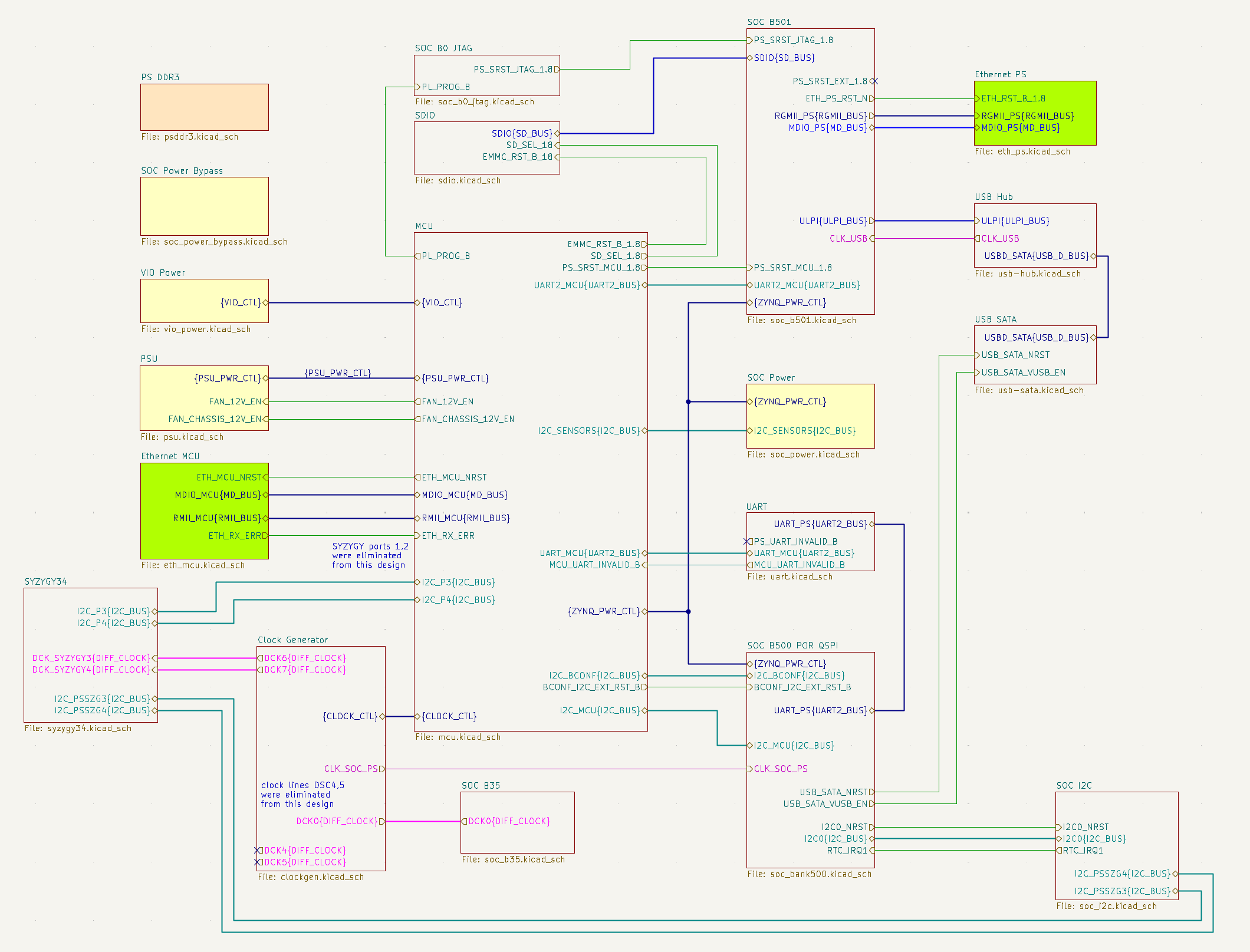
Design is made with KiCad 9. Below is a high-level overview of fundamental blocks.
Stackup
Cheapest 10-layer on JLCPCB - JLC10161H-2116(1.57mm±10%). That leaves me with quite fat tracks, but I think I can live with it.
SYZYGY
Why SYZYGY? What appeals to me is the relative simplicity compared to VITA 57 and the standard's open nature. What I dislike is the low count of differential pairs in STD port, so I've routed STD pins S16 and S18 as the ninth differential pair. With nine pairs, I can interface to ADCs and DACs using an 8-lane LVDS data bus, utilize bit-sync C2P pair defined by the standard, and use the ninth pair for frame sync. Initially, I planned to have 4 SYZYGY ports, but later reconsidered and left only two SYZYGY STD ports connected to HP banks. This leaves me with 1.8 to 1.2 volt VIO, which is fine with me. HP banks would allow much faster data throughput than HR, so the choice was obvious.
Base controller
The central part of the design sheet is occupied with a board base controller implemented on STM32H723 in a QFP package. QFPs are easy to troubleshoot because it's easy to solder a probe wire in, and they were the cheapest option. MCU controls not only SYZYGY ports via I2C, but also the selection of SOC boot media and a secondary PSU that powers up the Zynq SOC. MCU is connected to the SOC with a UART pair, so I can implement an IPMI with a remote boot console if I want to. It is also connected to ADCs that read the SOC's power consumption from shunt resistors and a couple of thermometers. STM32H723 is quite powerful, so I'm planning to use Zephyr OS and implement a web server for remote control.
ATX Power supply
I hate barrel jacks, period. ATX can provide more power than I ever need for both the carrier board and plugin pods. It also provides "power good" signal, 5V standby supply for the base controller, and can be switched on by connecting pin 16 of ATX motherboard connector to ground. It's a beautiful, standardized, cheap, and widely available option. It's got some switching noise, but I'm going to block it with Murata's BNX022-01L filter blocks. If I ever need a 12V supply for a transmitter pod, ATX provides a nice power extension for magnetic HDDs. All of the reasons above conclude my platonic feelings toward ATX. Let's see if they'll survive the harsh reality.
Secondary PSU
The SOC requires five different power supplies. Instead of designing my own, I have ripped off Digilent's ZYBO PSU schematics and followed (not very accurately) the manufacturer's recommendations on ADP5052 routing. Let's hope this won't create too much interference.
VIO Power
The VIO range is 1.8 .. 1.2V. Its design is inspired by Greg Davill's Butter Stick. VIO works in the TI Tina simulation. Let's see if it actually works.
Management Ethernet
The base controller got its own dedicated 10/100 Ethernet port for remote management. I've tried the Zephyr web server example on the STM32 Discovery, and it worked fine. Hoping it works on my board too.
SOC
Zynq XC7Z030. Why not XC7Z020? Because the XC7Z030 got more distributed RAM resources and bigger balls - literally... The ball pitch is 1mm, so that I can place a pair of 0.9mm traces between them with minimal effort.
DDR3
The two DDR3L chips are used in a fly-by topology, creating a 32-bit wide RAM data bus. Here comes the pain. I have no prior experience with multi-chip DDR3 RAM, and KiCad offers only length tuning. JLC10161H-2116 microstrip tacks are unacceptably fat with a 40 Ohm impedance. That's why I cross my fingers in hope that 50 Ohm tracks will work. If I hadn't screwed up the pin assignments and the SI "eye" stays open despite my non-orthodox PCB design practices, it might work.
Clock Generator
I've made the clocks as configurable as possible and chose TI's LMK03328RHSR double-PLL chip, which can work with two reference clock sources and generate the extra-low jitter signals with configurable amplitude. The primary clock source is a ECS-TXO-32CSMV-270 TCXO, and the secondary is an external clock input. If the balun on the external clock input is connected correctly, the external reference input may actually work. Why not use TCXO directly? Clocking wizards aren't very flexible, but an external chip is. The LMK03328RHSR is much more stable and has lower jitter. It is also more expensive, but I decided to pay slightly more to avoid headaches later during the block design phase. Of course, if it works as expected :)
SOC Boot Media
SOC can boot from JTAG, onboard QSPI, or a multiplexer connected to either an 8GB EMMC or a Micro-SD card. Boot media choice is controlled with I2C expander connected to the MCU base controller. MCU also controls EMMC/Micro-SD mux.
SOC Ethernet
Nothing fancy, just a cheap RTL8211 1Gb copper Ethernet PHY.
SOC USB
The SOC accesses USB 2.0 bus via USB3320C ULPI transceiver which is connected to CY7C65632 USB hub. One of the hub's ports goes to the standard USB2-A connector. The other one is connected to the USB-SATA controller.
SOC USB to SATA controller
Yes, I wanted an SSD disk! What I didn't like was spending a lot of time figuring out PCIe or SATA connectivity from the SOC to the SSD. USB-to-SATA is a nice compromise. We'll see that.
External UART
Both SOC and MCU have dedicated UART ports routed to venerable RS-232 DB9 sockets. This is so very convenient for rack-mounted gear and remote tests.
JTAG ports
The MCU and the SOC have JTAG sockets.
I think I've covered all of the peripherals. Now you can bet on the odds of bringing the very first edition of the board up to the Linux tty prompt.
GitHub
Finally, link to the repo: