NASR-M board bring-up, DDR3 test
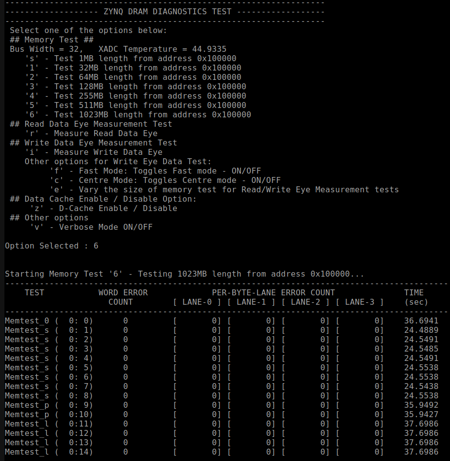
Today is an important milestone in a board bring-up, as the DDR3 subsystem appears functional. I was able to run a Vivado bundled Zynq bare-metal DDR test with no errors. The test image was uploaded via JTAG and executed on a CPU core.
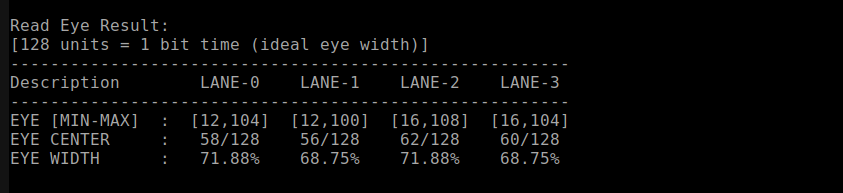
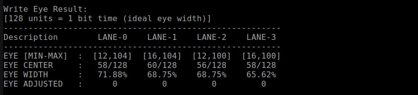
That was the most important indication of a system's health to me. Even if other subsystems don’t work properly, I’ll be able to respin the board with minimal effort. There are a few things to improve. Most importantly, the data strobe line length. Currently, the propagation delay between the strobe and data lines is very short, less than 0.01 nanoseconds. I suppose that contributed to somewhat narrow write eye width.
But hey, 65-71% is still ok, and definitely acceptable for a first prototype. Even without post-routing simulations, I’ve got a nice result. This routing won’t win the beauty contest, but at least it works, and someone may find it useful. Learn from my mistakes, kids :)
I’ve seen a lot of requests on the forums regarding fly-by topology applied to Zynq 7000, so here are a few tips and rules of thumb that worked for me:
First and most important one, read UG933 Zynq-7000 SoC PCB Design Guide.
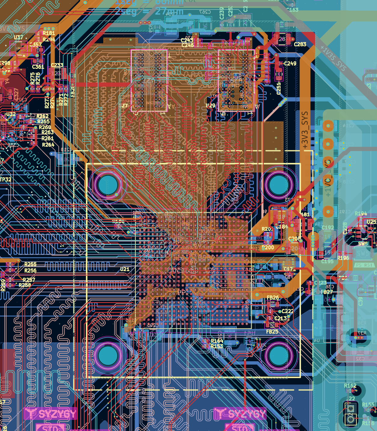
Keep continuous ground planes around command, control, and address lines. I have routed them all inside the inner layers. Layer In3 had no continuous ground above, so I drew a large ground polygon (an orange ballet dancer with Elvis hair) on layer In2 to sandwich the inner DDR lines.
The data and data strobe tracks are on the outer layers because they needed to be faster than the address and control lines.
Keep data strobes longer than data lines, and try to account for the delay rather than the length. I haven’t done that correctly, but I will improve it in the next design.
Use stitching between the ground layers, and don’t route the tracks near the voids. See UG933 for details.
Keep 3 to 5 track widths around the lines.
Avoid crossing layers. I was able to avoid it completely except for the termination resistor tracks.
The signal delay calculations are here: DDR timins spreadsheet
The complete design is available here: NASR-M
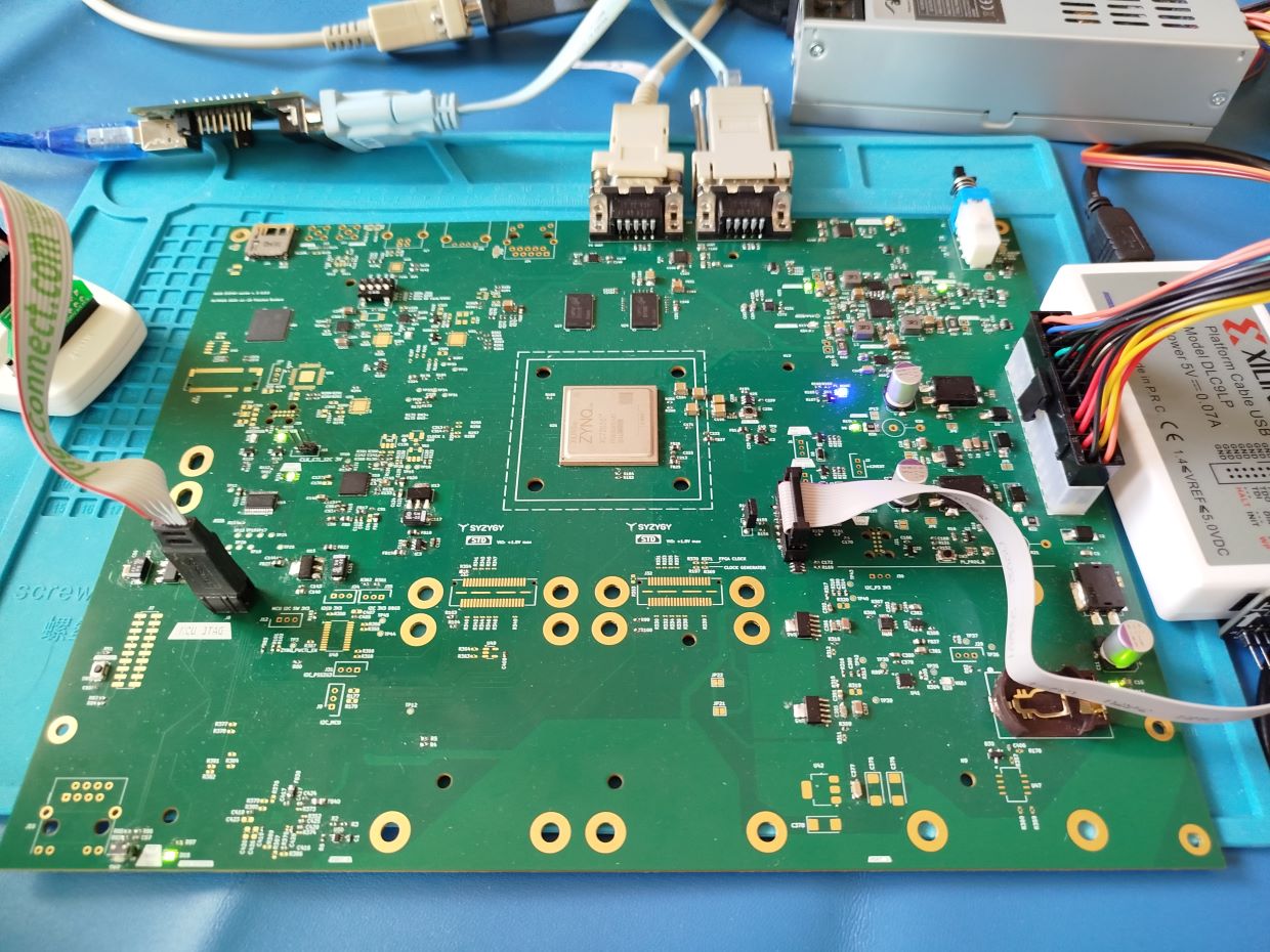
Finally, a small gallery of trophies to manifest my victory. Nerds have needs ... they love to brag about their dorky triumphs. I am not an exception.