NASR-M board bring-up, LMK03328 clock Zephyr OS driver
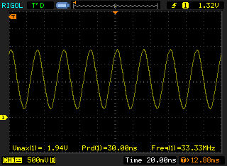
The LMK03328 clock driver is finally functional. Today, I was happily observing a sine-like signal at 33.33 MHz on the screen of my good old scope. I suppose it’s really a meander. Once I get a faster oscilloscope, I’ll be able to tell with confidence. What disappointed me was the low amplitude. The peak value was around 1.76 - 1.8V despite the 3.3V at the line #3 IO supply. The datasheet of LMK03328 states the following: “The 1.8-V LVCMOS driver supports rail-to-rail output swing only when powered from VDDO = 1.8 V +/- 5% (recommended VDDO for use with LVCMOS output format). VOH level is NOT rail-to-rail for VDDO = 2.5 V or 3.3 V due to the dropout voltage of the output channel’s internal LDO regulator.”
My expectation for peak amplitude was 2V or a little more. Let’s hope it's enough to clock the SOC. The driver for Zephyr OS is in a NASR-M-ZFW source tree. It’s a really simple one. First, it reads the register values described in a DTS, and then transfers them via the I2C. It works for me, and frankly speaking, I don’t want to spend any more time on this. At first, I tried to transfer the entire register config generated by TICS Pro, but that didn’t work. After a few tries, I had to cut out all register definitions that weren't related to the PLL or outputs, and it finally worked as expected.
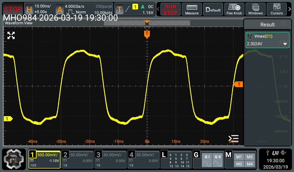
Update The clock signal amplitude is ok. My oldie scope was not able to display the fast rising signal correctly. Here is the oscillogram made with a faster scope.
Here is a DTS example:
    lmk03328: lmk03328@54 {
    compatible = "ti,lmk03328";
    init-priority = <90>;
    reg = <0x54>;
    /*software-reset;*/    /* clear R12[7] after writing all registers */

    status = "okay";

    reg-values = <
           0x1D01  /* R29  enable AC coupling mode on a primary input*/
           0x0232  /* R2     addr=0x02  val=0x32 */
           0x0300  /* R3     addr=0x03  val=0x00 */
           0x0CDF  /* R12    addr=0x0C  val=0xDF */
           0x0D00  /* R13    addr=0x0D  val=0x00 */
           0x0E00  /* R14    addr=0x0E  val=0x00 */
           0x1800  /* R24    addr=0x18  val=0x00 */
           0x19F5  /* R25    addr=0x19  val=0xF5 */
           0x14FF  /* R20    addr=0x14  val=0xFF */
           0x15FF  /* R21    addr=0x15  val=0xFF */
           0x16FF  /* R22    addr=0x16  val=0xFF */
           0x1702  /* R23    addr=0x17  val=0x02 */
           0x1B58  /* R27    addr=0x1B  val=0x58 */
           0x1C28  /* R28    addr=0x1C  val=0x28 */
           0x1D03  /* R29    addr=0x1D  val=0x03 */
           0x1E0C  /* R30    addr=0x1E  val=0x0C */
           0x1F20  /* R31    addr=0x1F  val=0x20 */
           0x2030  /* R32    addr=0x20  val=0x30 */
           0x2127  /* R33    addr=0x21  val=0x27 */
           0x2230  /* R34    addr=0x22  val=0x30 */
           0x237C  /* R35    addr=0x23  val=0x7C */
           0x2427  /* R36    addr=0x24  val=0x27 */
           0x2510  /* R37    addr=0x25  val=0x10 */
           0x262F  /* R38    addr=0x26  val=0x2F */
           0x2710  /* R39    addr=0x27  val=0x10 */
           0x282F  /* R40    addr=0x28  val=0x2F */
           0x2950  /* R41    addr=0x29  val=0x50 */
           0x2A0E  /* R42    addr=0x2A  val=0x0E */
           0x790F  /* R121   addr=0x79  val=0x0F */
           0x7A0F  /* R122   addr=0x7A  val=0x0F */
           0x7B0F  /* R123   addr=0x7B  val=0x0F */
           0x7C0F  /* R124   addr=0x7C  val=0x0F */
           0x2B50  /* R43    addr=0x2B  val=0x50 */
           0x2C0E  /* R44    addr=0x2C  val=0x0E */
           0x2D0A  /* R45    addr=0x2D  val=0x0A */
           0x2E00  /* R46    addr=0x2E  val=0x00 */
           0x2F00  /* R47    addr=0x2F  val=0x00 */
           0x30FF  /* R48    addr=0x30  val=0xFF */
           0x3205  /* R50    addr=0x32  val=0x05 */
           0x3303  /* R51    addr=0x33  val=0x03 */
           0x3400  /* R52    addr=0x34  val=0x00 */
           0x3500  /* R53    addr=0x35  val=0x00 */
           0x3600  /* R54    addr=0x36  val=0x00 */
           0x3700  /* R55    addr=0x37  val=0x00 */
           0x380E  /* R56    addr=0x38  val=0x0E */
           0x3915  /* R57    addr=0x39  val=0x15 */
           0x3A00  /* R58    addr=0x3A  val=0x00 */
           0x3B62  /* R59    addr=0x3B  val=0x62 */
           0x3C00  /* R60    addr=0x3C  val=0x00 */
           0x3D00  /* R61    addr=0x3D  val=0x00 */
           0x8407  /* R132   addr=0x84  val=0x07 */
           0x8505  /* R133   addr=0x85  val=0x05 */
           0x3E22  /* R62    addr=0x3E  val=0x22 */
           0x3F00  /* R63    addr=0x3F  val=0x00 */
           0x4000  /* R64    addr=0x40  val=0x00 */
           0x412D  /* R65    addr=0x41  val=0x2D */
           0x4203  /* R66    addr=0x42  val=0x03 */
           0x431A  /* R67    addr=0x43  val=0x1A */
           0x4403  /* R68    addr=0x44  val=0x03 */
           0x457D  /* R69    addr=0x45  val=0x7D */
           0x4607  /* R70    addr=0x46  val=0x07 */
           0x4712  /* R71    addr=0x47  val=0x12 */
           0x4818  /* R72    addr=0x48  val=0x18 */
           0x4900  /* R73    addr=0x49  val=0x00 */
           0x4A5A  /* R74    addr=0x4A  val=0x5A */
           0x4B00  /* R75    addr=0x4B  val=0x00 */
           0x4C00  /* R76    addr=0x4C  val=0x00 */
           0x4D00  /* R77    addr=0x4D  val=0x00 */
           0x5001  /* R80    addr=0x50  val=0x01 */
           0x510C  /* R81    addr=0x51  val=0x0C */
           0x5208  /* R82    addr=0x52  val=0x08 */
           0x5301  /* R83    addr=0x53  val=0x01 */
           0x5404  /* R84    addr=0x54  val=0x04 */
           0x5507  /* R85    addr=0x55  val=0x07 */
           0x5600  /* R86    addr=0x56  val=0x00 */
           0x5700  /* R87    addr=0x57  val=0x00 */
           >;
    };
Now that the clock works, I can start soldering the flash storage and supporting circuitry.